Indroduction
Both the Flash4 and Flash5 transmitters use the same circuit board, but only the Flash5 board has components installed for the trainer function. To provide trainer functions on the Flash4, you need to add some 25 components, as well as installing a switch and socket into the case.
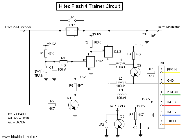
How it works
Transistor Q3 is normally turned on through resistor R7. The trainer cord has a link between pins 4 and 6 at the Student end. When the cord is plugged in, the base of Q3 will be shorted to ground. This turns the transistor off, disabling RF output. The PPM (Pulse Position Modulation) signal, which normally would be transmitted, is inverted by Q1 and sent out through pin 1 of the trainer cord. At the Master transmitter the PPM signal comes in through pin 2, and is un-inverted by Q2. The trainer switch selects transmission of either the Master's own PPM signal (via CMOS switch IC1/1), or the incoming signal from the Student (via IC1/3).Chokes L1-L3 and capacitors C1-C3 are added to prevent RF interference getting into parts of the circuit where it could cause misoperation.
None of this circuitry is present in a standard Flash4, but instead there are links at JP1 and JP2 (so it will always transmit its own PPM signal).
Components Required
| Qty | Description | Position |
| 2 | 100nF ceramic capacitor | socket |
| 2 | 1nF ceramic capacitor(smd) | C2,C3 |
| 6 | 100nF ceramic capicitor(smd) | C1,C4-C8 |
| 1 | 47K resistor(smd) | R1 |
| 1 | 100K resistor(smd) | R2 |
| 6 | 4K7 resistor(smd) | R3-R8 |
| 3 | 100uH choke | L1-L3 |
| 2 | BC846A NPN transistor(smd) | Q1,Q2 |
| 1 | BC337 NPN transistor | Q3 |
| 1 | CD4066 CMOS IC(smd) | IC1 |
| 1 | 6 pin 270° DIN socket | case |
| 1 | Momentary On toggle switch | SW1 |
Some substitutions are possible:- Q3 is an NPN transistor rated 150mA @ 20V or better. Q1 and Q2 are not critical, just about any NPN small-signal transistor of suitable size will do. For IC1 there are several equivalents available, such as 74C4066, MC14066, BU4066 etc.(make sure you get a high voltage part, not 74HC4066 or 74HCT4066 - these can only handle 5V). Chokes L1-L3 can be any coil valued at about 100uH (I used 150uH, because that's what I had at the time...).
NOTE: If you just want the trainer jack for controlling a computer flight-simulator, then only Q1, R5, R6 and L3 are required. Do not remove the links which connect JP1 and JP2. When using this simpler circuit, you should pull out the Tx crystal to stop RF output (as well as preventing possible RF interference, this greatly reduces current drain on the battery, so you can have much longer 'flights'!).
Installing the Trainer Upgrade
First you need to disassemble your transmitter. Pull out the crystal. Undo the 8 screws that hold the back on (including 2 in the handle), and remove the back. Unplug the battery wire. Unsolder the aerial wire, undo 4 screws holding the PCB, and extract the PCB from the case. The power switch knob will fall off - keep it in a safe place.
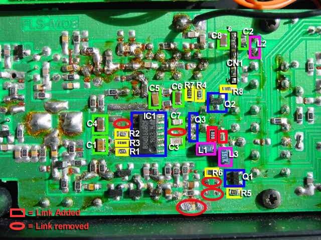
Several links must be removed from the PCB (some of these will be reused in the new circuit). A number of new parts have to be added, including the CD4066 quad bilateral CMOS switch, 3 transistors, 7 resistors, 8 capacitors, and 3 RF chokes. Most of the parts are SMD (Surface Mount Device) parts, which you solder onto the copper side of the PCB. Q3 and L1-L3 are installed through holes from the component side.
NOTE: C4-C8 are bypass capacitors which are not shown in the circuit diagram.
|
|
A six wire cable is required to connect from the PCB to the trainer jack. Route the cable under the PCB to the left-hand end of the case, then out to the jack on the back. Make it just long enough to reach the trainer socket when the back is off. You should twist the wires to reduce RF pickup.
|
|
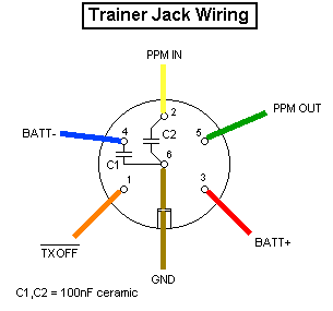
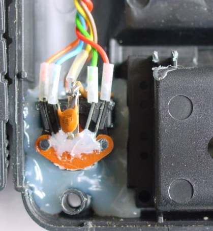
The trainer jack is a 6 pin, 270 degree DIN socket. The hole where the jack will be installed is covered by a round plastic bung. Cut this out and mount the jack, securing it with hot-melt glue or epoxy. Solder the two ceramic capacitors onto the jack, then connect the six wires from the PCB. The brown wire (GND) connects to both pin 6 and the shield tag.
If you want to use the Master function (for training another flyer) you need to drill a hole in the front panel and mount a switch there. The switch is then wired to Ground and to C1 (there is a hole in the PCB next to C1, for this purpose). A Momentary toggle switch is specified. Don't be tempted to use a switch that stays on by itself, as you might inadvertantly bump it and crash your plane before realising what went wrong! A switch with a long handle is better, as it is less tiring to hold operated.
Before re-assembling the radio, verify your wiring and component placement. Use a magnifying glass to examine the PCB for shorts or bad soldering. Don't try to operate the transmitter until you are 100% sure that everything is correct!